Adding vision to your projects needs not be a difficult task. Whether its machine vision for robot control or the sampling and storage of images for security, CMOS images sensors can offer many advantages over traditional CCD sensors. Just some of the technical advantages of CMOS sensors are,
No Blooming
Low power consumption. Ideal for battery operated devices
Direct digital output (Incorporates ADC and associated circuitry)
Small size and little support circuitry. Often just a crystal and some decoupling is all that is needed.
Simple to design with.
There are many manufacturers making CMOS Image Sensors. Just some of the more notable ones are Micron who acquired Photobit, OmniVision, ST who acquired VLSI Vision, Mitsubishi and Kodak.
There are two different categories of CMOS Sensors based on their output. One type will have a analog signal out encoded in a video format such as PAL, NTSC, S-Video etc which are designed for camera on a chip applications. With these devices you simply supply power and feed the output straight into you AV Equipment. Others will have a digital out, typically a 4/8 or 16 bit data bus. These 'digital' sensors simplify designs, where once a traditional 'analog' camera was feed into a video capture card for conversion to digital. Today, digital data can be pulled straight from the sensor.
The main components to a Digital Video Camera design are
CMOS Image Sensor. The heart of the camera. It produces a digital/analog output representing each pixel. It's support circuitry will normally include a Crystal Oscillator and power supply decoupling. Some sensors may need a resistive bias network of some type. All of these components are normally surface mounted on the back of the PCB and occupies very little real estate.
The lens Holder. This will be either a plastic or metal mount which attaches to your PCB and allows a standard size lens to be screwed in. The screw thread facilitates focusing for fixed lens systems. The base of the lens mount may also have a IR (Infra Red) filter.
The Lens. This will determine your Field of view among other things. Lenses range from fish-eye to telescopic and need to be purchased to fit the parameters of your sensor and lens holder.
Once you have completed the above, you have yourself a imaging system which constantly spits out a pixel data stream synchronised to a pixel, frame and/or line clocks. Connecting this directly to a microcontroller/processor system will cause headaches. Trying to clock this raw data in will use up great amounts of CPU time, if your uC could do it in the first place. If you drop a pixel because an ISR is doing some thing more privileged, then you have no ability to sample that location again, and thus no method of error correction.
While the frame rate on many devices can be slowed down by using internal divisors, it still doesn't reach an acceptable speed nor allow random access to pixels. Reducing the master clock rate of the device will effect exposure times and other time dependent settings, thus is not an option. Clearly some additional circuitry will need to be designed.
By using a CPLD/FPGA and RAM, you can program the CPLD to dump the data straight into RAM. Your micro could then read this RAM through the PLD which could be memory mapped. If you really want performance (And budget is not a problem), you could use Dual Port RAM. If however you only want to capture one frame, then the PLD could copy one frame into memory and ignore subsequent pixel data until an event such as when your device has read all the data out of RAM. Other options are to use a LVDS (Low Voltage Differential Signalling) serial bus, to relay your data over a few metres or more. At a high enough clock rate, you won't wait all day for a frame.
The other thing you must not forget is how to control the sensor. Most of it's internal parameters are controlled by a serial bus, typically I2C for the majority of sensors. This can either be controlled through a memory mapped Register programmed into your PLD or via an I2C port straight from your uC. All up this makes quite a cheap way to capture video. Ideal for your Embedded Linux Systems.
OmniVision not only develops CMOS Image Sensors, but also support device ICs such as the OV-511 & OV-518 Advanced Camera to USB Bridge. OmniVision is one of the more popular manufacturers with devices such as the OV7910 NTSC/PAL Camera on a Chip being used in many small analog camera modules around the world. This would be the recommended starting point if you are starting out designing with CMOS Image Sensors.
YUV/YCbCr 4:2:2, RGB 4:2:2 or Raw 8 bit RGB Outputs
3.3V Core <>
LCC-48 Package
OmniVision and some third party vendors (e.g. COMedia) have evaluation modules for the OmniVision sensors. This allows you to get up to speed with the sensor, incorporating a PCB with de-coupling, a Lens and Lens Holder. The majority of the sensor's signals are broken out to a header which you can use to interface to your own designs. The evaluation modules in small quantities are normally much easier to obtain than the sensors themselves, and are typically cheaper as a result.
A picture of the M3188 Evaluation Module with the lens holder removed. The signals can be obtained from the 32 pin header on the top of the module
DIY Electronics (http://www.kitsrus.com) are just one outlet which sells the third party evaluation boards.
In August 2001 Kodak launched it's first two CMOS Images to its Kodak Digital Science range of image sensors. Kodak has been in the game of CCD Sensors for twenty plus years with a wealth of imaging expertise and research.
Mitsubishi have broken the pack, to produce smaller resolution sensors. These sensors can typically be used for a range of applications such as finger print sensing, motor detection, gaming, tracing of moving parts etc. Just one application is the new optical mice flooding the market place. They use a low resolution Image Sensor to track movement on a wide variety of surfaces.
Also unique to these sensors is in-built image processing. Both sensors can output edge enhanced or extracted data, making them ideal for tracking on small robots, industrial control etc. The sensors can also process 2D images into 1D. The output of each pixel is by the means of a analog potential, thus this must be fed into an ADC to return digital image data.
Micron Imaging has aquired Photobit Corporation and inherited its IP and Image Sensors. CMOS APS (CMOS active pixel sensor) was first created by a team of JPL engineers lead by Dr Eric Fossum. Dr Fossum is now Fellow at Micron Tecnology Inc. Micron's Product range can be sought from Micron's Product Matrix
Spectronix have used the ST Sensors in their RoboCam Series. ST also offer a couple of CoProcessors, a STV0657 Digital CoProcessor, a STV0672 USB CoProcessor and a STV0680 DSC (Digital Still Camera) CoProcessor. The DSC CoProcessor offers an RS-232 / USB Interface and on board SDRAM Storage.
The sensors have resolutions from VGA up to 10 Mpixels and some can run at 10,000 frames per second. By Pieter Willems (Product Applications, Engineer, Cypress Semiconductor)
High-speed CMOS image sensors are available in several types for a variety of markets, for use in general purpose, high end or custom high-speed cameras. Such cameras can be used for applications like scientific research, crash tests, high-speed scanning, machine vision and military research; all requiring high frame rate motion capturing.
The sensors have resolutions from VGA up to 10Mpixels and some can run at 10,000 full frames per second. The sensor architecture can consist of two halves, quadrants or one pixel array. The outputs can be parallel analog outputs, one digital 10 bitoutput or digital serial LVDS outputs. The outputs operate at speeds up to 50Msamples/s each, thus realizing a 5.5Gpix/sec pixel throughput. This is the highest reported continuous pixel throughput for an image sensor to date. Image quality is at least 10bit, so after digitization in the camera the data throughput can be 55Gbit/sec. The target applications always require a 6T snapshot pixel with a high sensitivity and high dynamic range. The sensitivity of these image sensors depends greatly on the pixel size. This results in very big pixels and thus very big custom image sensors for some specific applications. Internal multiplexing schemes allow random windowing with increased frame rate. When reducing the window size to a small ROI, the frame rate rises up to 170,000 frames/sec. Most sensors are realized in a 0.25 process.
Recent trends in high speed image sensors
Today CMOS is the technology preferred for high-speed imaging. In today's market we can clearly see three trends in high-speed image sensors; very high speed, feature integration on-chip and generic high-speed imagers.
Pixel rate is the product of resolution and frame rate, and it is advancing by huge proportions. Today we can announce an image sensor of 1024x1024 pixels, working at more than 5000 full frames per second. Taking 10-bit quality into account, this means a total data rate on camera level of 55Gbit/sec. To achieve this extremely high data rate on the sensor level, combined with high image quality and (typically for this type of application) a very high sensitivity, it is important to not only focus on the design with respect to correct schematics, but also making sure the whole layout is well balanced. This means that power lines need to be well-distributed and all parasitic effects, electrical and optical, on each node in the layout should be well controlled. The power budget requires the designs of low power modules to keep within the total power requirement.
Examples of applications for high speed image sensors.
A different trend, in high-speed imaging, is the integration of high-speed ADC's, sequencers, LVDS transmitters and correction algorithms on-chip. These imagers are generally inferior with respect to speed and sensitivity to the imagers above but compensate this with ease-of-use and system integration capabilities. A third type of imagers we see emerging in the market today are generic high-speed imagers. Older (simple) generic imagers with analog outputs or without on-board timing generation are being replaced by faster and more complex image sensors. These imagers allow generic high-speed cameras to be built in a short amount of time.
The pixel
Figure 1 shows the schematic of the pixel used in a typical high-speed image sensor, which is the so-called 6-transitor pixel. Important for this type of image sensor is the pipelined global shutter feature.
The global shutter, in which all pixels start and end light integration at the same time, is very important for a high-speed application to have a well controlled motion blur that is exactly the same for all pixels. This global shutter allows high-speed motion scenes to be frozen by the imager.
Figure 1: The pixel
A typical high-speed capture sequence can be seen in Figure 2 (a small bullet hitting a matchstick). The pipelined feature means that during the readout of the pixel array, the integration of light in the pixel for the next frame is ongoing. This is required to guarantee that the frame rate is independent of the integration time.
Figure 2: Typical high-speed capture sequence (bullet hits match stick)
To obtain the highest possible sensitivity, the photodiode, collecting the photo charge and converting this charge into a voltage, needs to be designed as small as possible to minimize its parasitic capacitance. Additionally, the fill factor of the pixel, meaning the open area in the pixel contributing to the light sensitive area needs to be as large as possible. Both features of a small photodiode and a large fill factor are achieved by implementing the N-well pixel patent, in combination with a P-well opening around the photodiode. Besides a high sensitivity, it is also important to have a pixel storagecapacitor that doesn't give any noise contribution, is well shielded from light and has a low leakage. This pixel architecture gives very good results with respect to storing the pixel signal during readout. The major disadvantage of this structure is the lack of fixed pattern noise correction in the pixel, which has to be done outside the image sensor.
Faster pixel rates
The metric for the speed of an image sensor is the product of resolution and frame rate, this gives the pixel rate of the sensor. In the very high-end, high-speed imaging market, this metric can never be high enough. In this market, customers are willing to build very complex cameras as long as the desired full frame rate is achieved. Figure 3 shows an image of a typical very high-speed application (car crash test).
These very high speeds are only achieved by using parallel analog outputs (up to 128 outputs) that impose an integration challenge for the camera system. The architecture of this type of imager is rather simple; 6T pixels in a pixel array which is optionally divided into quadrants, several parallel high-speed analog busses and parallel output amplifiers to drive the outputs.
Figure 3: High-speed imaging application: Car crash test.
No ADC's, sequencers or other on-chip image processing is present on these chips. The chip-wide analog busses make sure all parallel outputs can be used regardless of the partial image size in the x direction that is readout. This allows boosting frame rate when reading out partial images.
Ghosting An important issue with these very high-speed image sensors is "ghosting" in the x-direction. This is caused by the relative large RC constant of the chip-wide analog busses. As it takes long for the signal on the busses to settle within 10-bit accuracy, a portion of the information of the previous pixel can still be present on the current pixel. In the image this results in ghosting in the x-direction. This type of ghosting is difficult to correct during image post processing.
One technique for addressing this problem is to precharge busses shortly before every new signal. This ensures that all information about previous pixels is destroyed. This technique requires the generation of short precharge pulses. The pulses are used to short the analog bus to ground. Most of these imagers are made as custom products upon request of the customers as there is no real need for this type of very high-speed imagers as a generic product today. Custom specifications can range from VGA to 10Mpixel and from 500 fps to 10000 fps, with data throughput up to 5.5Gpix/s. In figure 4 a typical very high-speed image sensor architecture is shown. Two halves are read-out in parallel with each having 64 parallel analog outputs. This results in a total of 128 high-speed parallel analog outputs!
Figure 4: Architecture of a typical very-high-speed image sensor
Smaller and easier to design with In contradiction with the very complex (and big) camera systems built around the sensors in the previous section, there is an increasing demand in the market for smaller and easier to implement high-speed image sensors.
High-speed imagers are starting to get used in several consumer-like applications such as scanning, vision systems and holographic data storage. The figure below shows a typical holographic data storage application and the imager used in it.
Figure 5: Holographic data storge and its high-speed imager
These applications need a lot of the system functionality to be on-board the image sensor. That is why ADCs, timing generators, image processing and additional output stages are implemented on the chip. For these imagers the level of feature-implementation is equally important as the sensitivity and the speed. Most of these imagers are still made on custom request with specific features that help to simplify the custom high-speed camera design. The figure below gives a typical architecture of this type of high-speed imager. These imagers typically have only one clock input, a few power supplies and some synchronization pins. All other signals to read-out and expose the imager are generated on-chip.
Figure 6: Architecture of a typical high-speed image sensor with a lot of logic and additional features on-board
Generic high-speed image sensors A third kind of high-speed image sensor we see (and have seen the last years) in the market is the general-purpose high-speed image sensor. Its applications range from machine vision cameras to traffic monitoring, scientific motion capturing and crash test inspection. The first generic high-speed image sensors consisted only of parallel analog outputs and had no logic on-board (much like the very high-speed imagers we know today). These days however we see a lot of features being implemented on the chip itself to make sure the imager can be used in a lot of different applications (multiple slope, subsampling, binning, flipping, mirroring, gain, offset, and so on).
Today, high-speed global shutter image sensors are under development that will provide 1.3MPxl at 1000fps. Typically these image sensors have the pipelined snapshot shutter capability and multiple slope capability. The on-board features differ from sensor to sensor.
Figure 7: Variety of applications for which generic high-speed imagers can be used
There are several different types of high-speed image sensors which are needed to meet the needs of different markets today. Very high-speed imaging sensors are purely analog image sensors with very high frame rates and data throughput which require complex -- and therefore mainly custom -- camera design. High-speed imaging sensors with on-board features offer many specific on-board features which assists developers in building these imagers into high-speed cameras which are used for more consumer-oriented applications. Features are implemented upon request of the customer so these are also mainly custom designs.
Finally, generic high-speed image sensors combine the most common features of the image sensors above to create a general-purpose image sensor capable of serving in cameras across a wide range of applications. These image sensors are available today off the shelf. Market trends suggest that on-board features, data rate, and resolution will continue to rise. The real challenge for developers moving into the future will be to combine a very high data rate image sensor with many on-board features such as LVDS and image processing.
About the author Pieter Willems is working as a Product Applications Engineer at the image sensor business unit from Cypress semiconductor. He started his career in the engineering department from Fillfactory and moved to product management before being acquired by Cypress. He can be reached at fpw@cypress.com.
CCDs and CMOS image sensors are increasingly used in robotics. Autonomous robots utilize cameras to track objects and identify movement characteristics. Unmanned vehicles that competed in the 2007 DARPA Grand Challenge used cameras in conjunction with LIDAR to identify objects in the environment in order to safely drive through the course. In the DARPA Urban Challenge, cameras were used in order to identify curbs and lane lines to keep the unmanned vehicles within lanes as they moved through an urban environment.
CCDs and CMOS image sensors use photo-active regions to read light characteristics in order to generate images. They provide the capability for environmental analysis, navigation, object identification and tracking. CCDs use a lens to direct light onto an array of capacitors which develop a charge that is proportional to the intensity of the incoming light. This charge is then transported across the exposed region and converted to voltage. These voltages can be used to recreate the image.
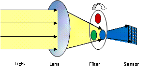
CMOS image sensors consist of an array of pixels built from transistors and a photodiode. The photodiode transforms the incoming light into a voltage. One transistor is used to reset the pixel for each image acquisition. Another serves as an amplifier so the signal is visible to the processing electronics. A third transistor is used as a switch so that a row of pixel voltages are sent to the processing electronics. Color information is recorded with one of two ways. One method is to use three sensors, each dedicated to detecting the intensity of one of the three primary colors. The three images are added together to create the final image. The second is to use filters to isolate the primary colors of the incoming light. The sensor makes three acquisitions, one for each primary color, and adds them together for the final image. For more information on camera sensors, refer to Anatomy of a Camera at ni.com/zone.
Figure 1. Image Sensor Setup to Capture Blue Component
Both image sensors can be used for most applications. However, there are advantages to both:
CCD
Higher quality images with little noise
Typically more pixels
Higher sensitivity to light
CMOS
Lower cost
Easier to build
Lower power consumption
Robotics applications using both CCD and CMOS image sensors can be implemented with LabVIEW and National Instruments products. Virginia Tech's team Victor Tango's entry in the 2007 DARPA Urban Challenge used LabVIEW to control their vision systems and analysis of image data. Drivers and software are available for both NI Vision products as well as third-party sensors including the Point Grey Research Firefly MV and Firefly 2. Refer to National Instruments Industrial Camera Advisor for more information on using third-party cameras with National Instruments hardware.
Name: Musa Home: Depok, Jawa Barat, Indonesia About Me: Seorang yg sederhana, moderat, individu serta suka dedikasi dan komitmen dalam semua aspek hidup. Dalam pandanganku sendiri sebagai seorang stabil, bertanggung jawab, percaya diri dan orang penuh kasih yang mempunyai niat baik. Kenangan dari segalanya langkahku merupakan pengalaman berharga dimasa mendatang. Petualanganku dimulai dari pulau “Celebes” yang lebih dikenal dengan Sulawesi. Tepatnya di daerah Gorontalo tempat kelahiran dan masa-masa kecilku bermain dan tumbuh.
Minat yang berkisar akademis terutama hardware system, petualangan. Mengunjungi suatu tempat dan hidup bebas dari “penjajahan” kesenangan penuh kasih.
Bagaimanapun, seorang Purnawarman Musa masih merasakan bahwa aku bukanlah seorang yang sempurna.