Suatu hari, ketika Nabi saw sedang berkumpul dengan para sahabat di dekat ka'bah, seorang lelaki asing lewat di hadapan mereka. Setelah lelaki itu berlalu, Nabi berujar kepada para sahabat, ''Dialah ahli surga.'' Dan hal itu dikatakannya sampai tiga kali.
Atas pernyataan Nabi tersebut, timbul penasaran di kalangan para sahabat, terutama Abdullah bin Umar yang memang dikenal sangat kritis. ''Ya, Rasulullah,'' tanya Abdullah, ''Mengapa engkau katakan itu kepada kami, padahal selama ini kami tidak pernah mengenalnya sebagai sahabatmu? Sedang terhadap kami sendiri yang selalu mendampingimu engkau tidak pernah mengatakan hal itu?'' Lalu sebagai seorang uswah, Nabi memberikan jawaban diplomatis yang sangat bijak. ''Jika engkau ingin tahu tentang apa yang aku katakan, silakan engkau tanyakan sendiri kepadanya.'' Karena rasa penasarannya sangat tinggi, suatu hari Abdullah bin Umar menyengajakan diri untuk berkunjung ke rumah orang asing itu.
''Ya, akhie,'' kata Abdullah, ''kemarin sewaktu engkau lewat di hadapan kami, Rasulullah mengatakan bahwa engkau seorang ahli surga. Apa gerangan yang menjadi rahasianya sehingga Rasulullah begitu memuliakanmu?'' Lelaki itu tersenyum, kemudian menjawab, ''Sesungguhnya aku tidak pernah melakukan apa-apa. Aku bahkan tidak memiliki kekayaan apa-apa. Baik ilmu maupun harta yang bisa kusedekahkan. Yang kumiliki hanyalah kecintaan. Kecintaan kepada Allah, kepada Rasulullah dan kepada sesama manusia. Dan setiap malam menjelang tidur, aku selalu berusaha menguatkan rasa cinta itu, sekaligus berusaha menghilangkan perasaan benci yang ada kepada siapa saja. Bahkan terhadap orang-orang kafir sekalipun.''
Memelihara perasaan benci dan marah, berarti menyimpan egoisme. Adanya perasaan benci, berarti adanya sikap untuk menyalahkan orang yang dibenci itu. Dan menyalahkan orang lain berarti membenarkan sikap dan tindakan sendiri. Padahal sikap semacam itu sudah sejak awal diklaim syetan pada penciptaan Adam as. Kisah tersebut memberikan gambaran kepada kita, bahwa perasaan benci, bukan hanya mengakibatkan fitnah dan permusuhan, tetapi juga dapat menimbulkan penyakit batin yang sangat fatal, sekaligus menjauhkan diri dari surga yang menjadi dambaan setiap mukmin. Sehingga sikap yang paling bijaksana adalah, selalu berusaha untuk mengintrospeksi diri, sekaligus menjadi orang yang pemaaf. Sebab itulah yang selalu dilakukan Nabi sepanjang perjalanan hidupnya. Sedangkan hidup Nabi adalah contoh bagi setiap mukmin. ahi
Rasa malu bagi seseorang merupakan daya kekuatan yang mendorongnya berwatak ingin selalu berbuat pantas dan menjauhi segala perilaku tidak patut. Orang yang memiliki watak malu adalah orang yang cepat menyingkiri segala bentuk kejahatan. Sebaliknya, yang tidak memiliki rasa malu berarti ia akan dengan tenang melakukan kejahatan, tidak peduli omongan, bahkan, cercaan orang lain. ''Anjing menggonggong kafilah tetap berlalu,'' begitu mottonya.
Islam menilai, watak malu itu merupakan bagian dari iman. Dengan demikian, orang yang tidak mempunyai rasa malu adalah orang yang hilang imannya. Orang hidup bermasyarakat sudah tentu harus mendengarkan apa kata masyarakat tentang dirinya. Masyarakat tak pelak lagi sebenarnya mengetahui apa yang dilakukan anggotanya. Masyarakat pula yang berhak mengoreksi apa-apa kelakuan yang tidak baik atau tak pantas anggotanya. Bagi yang tak punya malu, omongan atau koreksi masyarakat akan dianggapnya angin lalu.
Ada sebuah ungkapan warisan para nabi, yang menyatakan bahwa sudah rahasia umum, orang yang hilang perasaan malunya tak lain dari orang yang sudah terbiasa berbuat kemungkaran dan kemaksiatan dalam segala jenis dan bentuknya. Ia mau melakukan kejahatan, kelaliman dan kekejian.
Rasulullah bersabda: ''Sesungguhnya, yang dapat diambil sebagai pelajaran dari para nabi terdahulu ialah, apabila kamu sudah tidak mempunyai perasaan malu maka berbuatlah semaumu;'' riwayat Imam Bukhari dan Muslim. Itu berarti, orang yang demikian sulit untuk mau mawas diri, meski berhadapan dengan umpatan dan kecaman orang banyak pun.
Berdasar riwayat Ibnu Umar, Rasulullah bersabda: ''Sesungguhnya Allah yang Maha Mulia dan Maha Agung, bila berkehendak menjatuhkan seseorang maka Allah cabut dari orang itu rasa malunya. Ia hanya akan menerima kesusahan (dari orang banyak yang marah kepadanya). Melalui ungkapan kemarahan itu, hilang pulalah kepercayaan orang kepadanya.
Bila kepercayaan kepadanya sudah hilang maka ia akan jadi orang yang khianat. Dengan menjadi khianat maka dicabutlah kerahmatan dari dirinya. Bila rahmat dicabut darinya maka jadilah ia orang yang dikutuk dan dilaknati orang banyak. Dan bila ia menjadi orang yang dilaknati orang banyak maka lepaslah ikatannya dengan Islam.'' ahi
Adding vision to your projects needs not be a difficult task. Whether its machine vision for robot control or the sampling and storage of images for security, CMOS images sensors can offer many advantages over traditional CCD sensors. Just some of the technical advantages of CMOS sensors are,
No Blooming
Low power consumption. Ideal for battery operated devices
Direct digital output (Incorporates ADC and associated circuitry)
Small size and little support circuitry. Often just a crystal and some decoupling is all that is needed.
Simple to design with.
There are many manufacturers making CMOS Image Sensors. Just some of the more notable ones are Micron who acquired Photobit, OmniVision, ST who acquired VLSI Vision, Mitsubishi and Kodak.
There are two different categories of CMOS Sensors based on their output. One type will have a analog signal out encoded in a video format such as PAL, NTSC, S-Video etc which are designed for camera on a chip applications. With these devices you simply supply power and feed the output straight into you AV Equipment. Others will have a digital out, typically a 4/8 or 16 bit data bus. These 'digital' sensors simplify designs, where once a traditional 'analog' camera was feed into a video capture card for conversion to digital. Today, digital data can be pulled straight from the sensor.
The main components to a Digital Video Camera design are
CMOS Image Sensor. The heart of the camera. It produces a digital/analog output representing each pixel. It's support circuitry will normally include a Crystal Oscillator and power supply decoupling. Some sensors may need a resistive bias network of some type. All of these components are normally surface mounted on the back of the PCB and occupies very little real estate.
The lens Holder. This will be either a plastic or metal mount which attaches to your PCB and allows a standard size lens to be screwed in. The screw thread facilitates focusing for fixed lens systems. The base of the lens mount may also have a IR (Infra Red) filter.
The Lens. This will determine your Field of view among other things. Lenses range from fish-eye to telescopic and need to be purchased to fit the parameters of your sensor and lens holder.
Once you have completed the above, you have yourself a imaging system which constantly spits out a pixel data stream synchronised to a pixel, frame and/or line clocks. Connecting this directly to a microcontroller/processor system will cause headaches. Trying to clock this raw data in will use up great amounts of CPU time, if your uC could do it in the first place. If you drop a pixel because an ISR is doing some thing more privileged, then you have no ability to sample that location again, and thus no method of error correction.
While the frame rate on many devices can be slowed down by using internal divisors, it still doesn't reach an acceptable speed nor allow random access to pixels. Reducing the master clock rate of the device will effect exposure times and other time dependent settings, thus is not an option. Clearly some additional circuitry will need to be designed.
By using a CPLD/FPGA and RAM, you can program the CPLD to dump the data straight into RAM. Your micro could then read this RAM through the PLD which could be memory mapped. If you really want performance (And budget is not a problem), you could use Dual Port RAM. If however you only want to capture one frame, then the PLD could copy one frame into memory and ignore subsequent pixel data until an event such as when your device has read all the data out of RAM. Other options are to use a LVDS (Low Voltage Differential Signalling) serial bus, to relay your data over a few metres or more. At a high enough clock rate, you won't wait all day for a frame.
The other thing you must not forget is how to control the sensor. Most of it's internal parameters are controlled by a serial bus, typically I2C for the majority of sensors. This can either be controlled through a memory mapped Register programmed into your PLD or via an I2C port straight from your uC. All up this makes quite a cheap way to capture video. Ideal for your Embedded Linux Systems.
OmniVision not only develops CMOS Image Sensors, but also support device ICs such as the OV-511 & OV-518 Advanced Camera to USB Bridge. OmniVision is one of the more popular manufacturers with devices such as the OV7910 NTSC/PAL Camera on a Chip being used in many small analog camera modules around the world. This would be the recommended starting point if you are starting out designing with CMOS Image Sensors.
YUV/YCbCr 4:2:2, RGB 4:2:2 or Raw 8 bit RGB Outputs
3.3V Core <>
LCC-48 Package
OmniVision and some third party vendors (e.g. COMedia) have evaluation modules for the OmniVision sensors. This allows you to get up to speed with the sensor, incorporating a PCB with de-coupling, a Lens and Lens Holder. The majority of the sensor's signals are broken out to a header which you can use to interface to your own designs. The evaluation modules in small quantities are normally much easier to obtain than the sensors themselves, and are typically cheaper as a result.
A picture of the M3188 Evaluation Module with the lens holder removed. The signals can be obtained from the 32 pin header on the top of the module
DIY Electronics (http://www.kitsrus.com) are just one outlet which sells the third party evaluation boards.
In August 2001 Kodak launched it's first two CMOS Images to its Kodak Digital Science range of image sensors. Kodak has been in the game of CCD Sensors for twenty plus years with a wealth of imaging expertise and research.
Mitsubishi have broken the pack, to produce smaller resolution sensors. These sensors can typically be used for a range of applications such as finger print sensing, motor detection, gaming, tracing of moving parts etc. Just one application is the new optical mice flooding the market place. They use a low resolution Image Sensor to track movement on a wide variety of surfaces.
Also unique to these sensors is in-built image processing. Both sensors can output edge enhanced or extracted data, making them ideal for tracking on small robots, industrial control etc. The sensors can also process 2D images into 1D. The output of each pixel is by the means of a analog potential, thus this must be fed into an ADC to return digital image data.
Micron Imaging has aquired Photobit Corporation and inherited its IP and Image Sensors. CMOS APS (CMOS active pixel sensor) was first created by a team of JPL engineers lead by Dr Eric Fossum. Dr Fossum is now Fellow at Micron Tecnology Inc. Micron's Product range can be sought from Micron's Product Matrix
Spectronix have used the ST Sensors in their RoboCam Series. ST also offer a couple of CoProcessors, a STV0657 Digital CoProcessor, a STV0672 USB CoProcessor and a STV0680 DSC (Digital Still Camera) CoProcessor. The DSC CoProcessor offers an RS-232 / USB Interface and on board SDRAM Storage.
THE PURPOSE of this primer is to introduce the technology used in CMOS image sensors as well as promoting a better understanding of the consumer product potential unleashed as the Internet, digital imaging and integrated information appliances converge. It is assumed that the reader is familiar with some basic physics and semiconductor technology, but most of this overview covers entry level imaging technology information.
THIS DOCUMENT starts with the basics of light and builds on this information to bring an understanding of CMOS imagers. Also included are some terms and phrases you may run into in the digital imaging industry.
Visible light is the band of electromagnetic radiation that can be sensed by the human eye. Electromagnetic radiation is the type of energy, traveling in a wave that is produced by an oscillating charge or energy source. Electromagnetic ("EM") waves also include radio waves, x-rays and gamma rays.
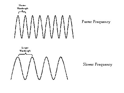
An electromagnetic wave can be defined by its wavelength (measure of length peak-to-peak) or its frequency (number of cycles per second). The multiplication of these two characteristics is a constant - the speed of light - so the two are inversely proportional to one another. That is, the shorter the wavelength, the faster the frequency, the longer the wavelength, the slower the frequency.
Visible light is usually referred to in wavelength (instead of frequency) and includes wavelengths of 400 nanometers (10 -9 meters, abbreviated "nm") to 750 nm. Ultraviolet and infrared refer to the wavelengths just beyond the ends of the visible electromagnetic spectrum:
Wavelength Band
Type of Radiation
Frequency (cycles per second)
~10 -14 meters
Gamma Rays
~10 22
~10 -9 meters (nanometer)
X Rays
~10 17
~10 -7 meters
Ultraviolet
~10 15
~10 -6 meters
Visible Light
~10 14
~10 -5 meters
Infrared
~10 13
~10 -2 meter (centimeter)
Short Wave Radio
~10 10
~1 meter
TV and FM Radio
~10 8
~10 2 meters
AM Radio
~10 6 (megahertz)
~10 6 meters
Long Wave Radios
~10 2
Measurements approximate. The product of the wavelength times the frequency equals 3x10⁸ meters per second, the speed of light.
Everyday usage of this chart is heard in the terms "short wave radio" and "900MHz cordless phone".
Photons
While light has properties of waves, the energy carried by light is not distributed in a wave, but carried in discrete bundles (or "quantized"), giving light some properties like particles. These light "particles" are called photons, and are referred to when explaining how light transfers energy and are used to explain how CMOS Imagers transfer light energy to electrical energy.
Color
The Visible Light band in the EM spectrum can be broken down into a series of colors, each color corresponding to a different wavelength. The typical spectrum that is displayed is seven colors - red, orange, yellow, green, blue, indigo, and violet. In reality the band represents a continuum of colors, each corresponding to a different wavelength, but seven colors are historically displayed. The bands outside this region - ultraviolet and infrared - are said to be beyond the range of the human eye, although in experiments both ultraviolet and infrared light can be seen unaided in certain conditions.
Visible Band
400nm
500nm
600nm
The Human Eye
The human eye can discriminate between hundreds of wavelengths as well as the intensity of the light source being received. The ability to distinguish these characteristics is through two main types of sensory cells in the retina:
rods - Rods convert photons into an electrical impulse that is processed by the brain. Rod cells are stimulated by the intensity of light and are responsible for perceiving the size, shape, and brightness of visual images. They do not perceive color and fine detail; tasks performed by the other major type of light-sensitive cell, the cone. The rods are what are in use when you are in the dark, meaning a red stop sign looks gray when you look at one without the aid of your car's headlights.
cones - Cones are less sensitive to low illumination levels, but give us our color vision. There are three types of cones, each of which contains a distinctive type of pigment. One cone absorbs red light, another green, and the third type blue. A given color stimulates all three types of receptors with varying effectiveness; the pattern of these responses determines the color perceived. This color breakdown is explained more in color reproduction, below.
The mnemonic to remember which cells does what is that Cones receive Color and both start with a "C"! Rod cells are not only much more sensitive to light than cones but are also much more numerous. The human eye contains about 130 million rods to about 7 million cones. This means that the human eye is much more sensitive to the intensity of the light than its color. This characteristic is taken advantage of in color processing, which will be covered later.
Color Mixing and Reproduction
This basic problem of color reproduction comes down to the question of how to create all the colors that are possible in the color spectrum. Over the years, it has been discovered that all the colors in the spectrum can be recreated from only a sub sample of only three other colors by mixing them in varying degrees.
The fact that the whole range of colors may be synthesized from only three primary colors is essentially a description of the process by which the eye processes colors. This is a fortunate property of vision since it allows three colors to represent any of the 10,000 or more colors (and brightness) that may be distinguished by human vision. If this was not the case and vision was dependent on the energy and wavelength relationship of light described above, it is doubtful that color reproduction could be incorporated in any mass-communication system.
The three main ways to reproduce color are as follows:
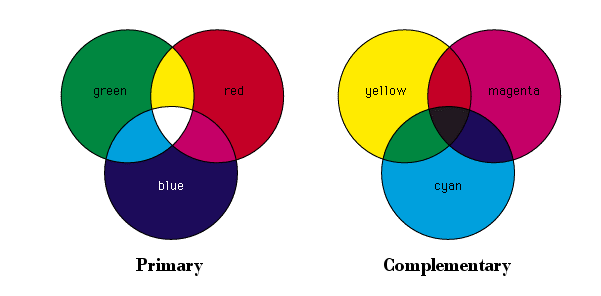
Primary Colors - Red, Green, Blue or "RGB" - Most people remember this from their childhood art classes. This is an "additive" method of adding the three primary colors in different amounts to recreate other colors, usually used in systems that project light. A mixture of these three primaries - red, green, and blue - may match any other color if their relative intensities are varied. White is made by adding ALL the colors (remember that "white light" represents the entire visible EM spectrum). The RGB scheme is used by televisions, computer monitors and other devices that project with light.
Complementary Colors - Cyan, Magenta, Yellow or "CMY" - This method is "subtractive" and is primarily used in printing since ink pigment "subtracts" the light falling on it. For example, a yellow pigment "absorbs" blue and violet light and "reflects" yellow (along with green and blue which together make more yellow). Since RGB is the best method for adding colors, then "negative red", or a pigment which absorbs the most red, "negative green", or a pigment which absorbs the most green, and "negative blue", which absorbs the most blue, are the best colors for subtracting. These colors, respectively, are Cyan, Magenta and Yellow. This method is used in inkjet printers and other methods that print (rather than project, which uses RGB). In practice, most inkjet printers not only use C, M, and Y ink, but also black ink since black, the combination of all the colors, would use up those inks very quickly. Since "B" already means "Blue", the last letter of the word "black" is used, meaning this method is referred to as "CMYk". Subtractive filters are used in consumer cameras since they absorb less light. Professional cameras use additive filters since additive produces more accurate color.
YCRCB - Luminance, Chrominance (Red), Chrominance (Blue) - The third way to characterize light makes use of the RGB concept above, but breaks down the color components in different fashion. Any color can be broken down into two qualities:
Luminance - Its brightness or intensity. Remember that the human eye that is more sensitive to brightness than to color. The luminance value, stated with the letter "Y", is the brightness breakdown of the color.
Chrominance - the color "remaining" once luminance is removed. This can be broken down again into two independent qualities:
Hue - This is the color of the light, in this case red or blue.
Saturation - the relative purity, or the amount of white light mixed with a hue. High saturation colors contain little or no white light.
The translation from RGB to YCRCB is done with a "look-up table" which takes any RGB value and matches it to its corresponding YCRCB components.
Binary Representation of Pictures
The fact that color can be broken down into individual components is extremely important to digital imaging - the process of breaking down a picture into the "1"s and "0" of digital communications. The process of breaking down a picture into individual components can be done in two basic steps:
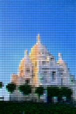
Breaking down the picture into a pixel grid - For a picture to be described as a series of 1s and 0s, it first must be broken down into a grid, or array. This process simply places a grid over a picture and assigns a single color for each square in the grid. This single color grid square is called a "pixel" (short for picture element).
The number of pixels used for the picture breakdown is called the "spatial resolution" and is usually referred to by its horizontal and vertical number of pixels, such as "640x480", meaning 640 pixels horizontally and 480 pixels vertically.
For a given picture, the number of pixels will determine the quality of the digital picture. That is, the smaller number of pixels, the larger they must be and the lower the picture quality. The higher number of pixels, the smaller each pixel is and the better the picture quality:
Low Spatial Resolution
High Spatial Resolution
Large Pixel Size Fewer Pixels Low Picture Quality
Small Pixel Size More Pixels High Picture Quality
Standard Spatial Resolutions
There are a number of standard resolutions, or arrays, in the sensor industry. Most of these formats come from the display monitor industry, which drives the number of pixels you see on computer monitors. Since sensors typically display on monitors, they commonly match monitor resolutions. Term one will hear in regards to spatial format include:
CIF - Common Intermediate Format - 352 x 288 pixels for a total of 101,376 pixels (commonly referred rounded at 100,000 pixels). This format was developed for PC video conferencing. The number of pixels is fairly small, but was needed in order to get full motion video at 30 frames per second.
QCIF - Quarter CIF - One quarter of a CIF format, so 176x144 for a total of about 25,000.
VGA - Video Graphics Array - 640x480 pixels for a total of 307,200 pixels. The VGA format was developed for computer monitors by IBM and become the standard for monitors for many years. Although monitor resolutions today are higher, VGA is still lowest "common" display which all PCs will support.
SVGA - Super VGA - 800x600 pixels for a total of 480,000 pixels. The next highest monitor resolution developed for PCs.
XGA - "Xtended" Graphics Array - 1024x768 for a total of 786,432 pixels. Another monitor standard.
If a sensor is not one of these standards, its resolution is simply displayed as vertical by horizontal (200x300, for example). Typically, if a sensor has more than 1 million total pixels (anything more than 1000x1000 pixels), it is termed a "megapixel" sensor, which has come to mean any sensor with more than one million pixels.
Digital Representation of Pixels
Now that the picture is represented as an array of pixels, each pixel needs to be described digitally. To do this, each pixel is assigned two main components: its location in the picture and its color. Its location is usually just represented by its "x and y" coordinate in the grid. Its color is represented by its color resolution, which is the method of describing a color digitally.
Using the RGB method of color representation, a color can be divided into an arbitrary number of levels of that color. For example, red can be broken down from total red to no red (or white):
No Red
Total Red
Each step in the arbitrary breakdown is called a "gray level" (even though the color is not gray). The same breakdown can be done for green and blue.
By experiment, the naked eye can distinguish about 250 shades of each color. Using binary math, the closest binary number is 256, which is 28, gray levels can be used for each color. This means for each color component of a picture, there are 8-bits used for each R, G, B element, for a total of 24 bits of color representation. The complete R, G, breakdown of 224 colors represents about 16.7 million colors that can be represented digitally. The number of colors represented by a pixel is called its "tonal resolution" or its "color dynamic range". If fewer bits are used, the number of colors represented is smaller, so its dynamic range is smaller.
Image Sensors
Image sensors are devices that take an image and directly convert it to a digital image. Referred to in marketing literature as "silicon firm" or "silicon eyes", these devices are made of silicon since silicon has the properties of both being sensitive to light in the visible spectrum and being able to have circuitry integrated on-board. Silicon image sensors come in two broad classes:
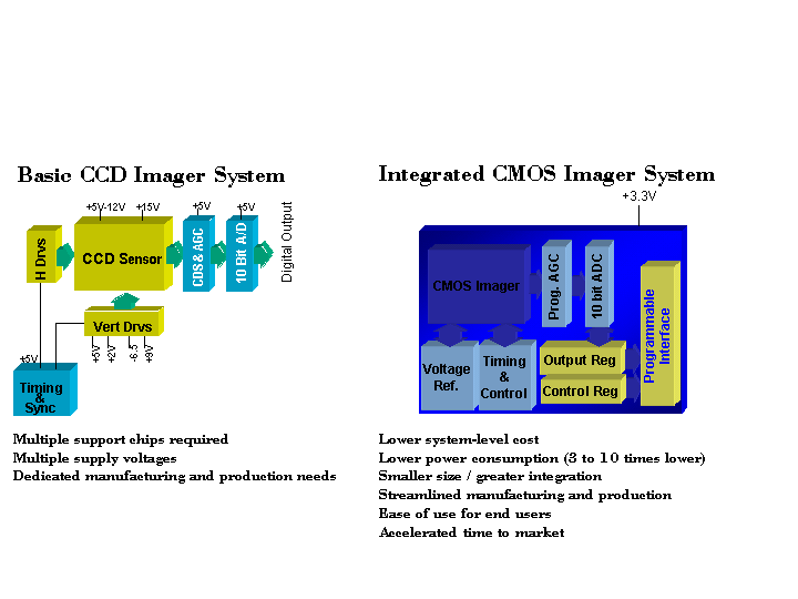
Charge-Coupled Devices (CCD) - Currently the most commonly used image sensor, CCDs capture light onto an array of light-sensitive diodes, each diode representing one pixel. For color imagers, each pixel is coated with a film of red, green, or blue (or complementary color scheme) so that each particular pixel captures that one particular color.
The pixel, made up of a light sensitive diode, converts the light photon into a charge, and the value of that charge is moved to a single location in a manner similar to a row of people passing buckets of water. At the end, the charge is amplified. Since this "bucket brigade" is accomplished by applying different voltages to the pixels in a succession, the process is called charge-coupling. Because the value in the pixel is moved by applying different voltages, CCD sensors must be supported by several external voltage generators. In addition, CCDs require a specialized manufacturing process that cannot be used by any other device.
Graphical representation of CCD
Image source: Digital Photography Review
CMOS Imagers - Like CCDs, these imagers are made from silicon, but as the name implies, the process they are made in is called CMOS, which stands for Complementary Metal Oxide Semiconductor. This process is today the most common method of making processors and memories, meaning CMOS Imagers take advantage of the process and cost advancements created by these other high-volume devices.
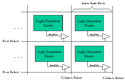
Like CCDs, CMOS imagers include an array of photo-sensitive diodes, one diode within each pixel. Unlike CCDs, however, each pixel in a CMOS imager has its own individual amplifier integrated inside. Since each pixel has its own amplifier, the pixel is referred to as an "active pixel". (note: There are also "passive pixel sensors" (pps) that do not contain this amplifier). In addition, each pixel in a CMOS imager can be read directly on an x-y coordinate system, rather than through the "bucket-brigade" process of a CCD. This means that while a CCD pixel always transfers a charge, a CMOS pixel always detects a photon directly, converts it to a voltage and transfers the information directly to the output. This fundamental difference in how information is read out of the imager, coupled with the manufacturing process, gives CMOS Imagers several advantages over CCDs.
CMOS Sensor Array
CMOS vs. CCD
Due to both design and manufacturing considerations, there are a number of advantages that CMOS Imagers have over CCD:
Integration - Because CMOS Imagers are created in the same process as processors, memories and other major components, CMOS Imagers can integrated with these same components onto a single piece of silicon. In contrast, CCDs are made in a specialized process and require multiple clocks and inputs. This feature limits CCDs to discrete systems, which in the long run will put CMOS Imagers at a cost advantage, as well as limit what kinds of portable devices CCDs can be integrated into.
Reduced Power Consumption - because of all the external clocks needed to "bucket brigade" each pixel, CCDs are inherently power hungry. Every clock is essentially charging and discharging large capacitors in the CCD array. In contrast CMOS imagers require only a single voltage input and clock, meaning they consume much less power than CCDs, a feature that is critical for portable, battery operated devices.
Pixel Addressibility - CCDs use of the bucket brigade to transfer pixel values means that individual pixels in a CCD cannot be read individually. CMOS imagers on the other hand have the pixels in an x-y grid allowing pixels to be read individually. This means that CMOS imagers will be able to do functions such as "windowing", where only a small sample of the imager is read, image stabilization to remove jitters from camcorders, motion tracking and other advanced imaging techniques internally that CCDs cannot do.
Manufacturing Cost - Since CMOS imagers are manufactured in the same process as memories, processors and other high-volume devices, CMOS imagers can take advantage of process improvements and cost reductions these devices drive throughout the industry.
CMOS Imager Characteristics
There are a number of phrases and terms for describing the functional capability, physical features or competitive characteristics of an imager:
Active Pixel Sensor (also APS) - As explained above, an active CMOS Imager pixel has its own amplifier for boosting the pixel's signal. Active Pixels are the dominant type of CMOS Imagers in the commercial market today. The other type of CMOS Imager, a passive pixel sensor (PPS), consists of only the photo detector without a local amplifier. While very sensitive to low light conditions, these types of sensors are not suitable for commercial applications due to their high amount of noise and poor picture quality when compared to active pixels.
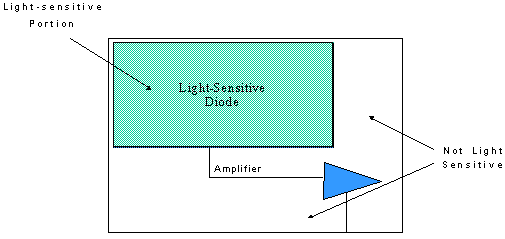
Fill Factor - The amount of a CMOS Pixel that is actually capturing light. In an active pixel, both the photo detector and the amplifier take up "real estate" in the pixel. The amplifier is not sensitive to light, so this part of the pixel area is lost when taking a picture.
The fill factor is simply the percentage of the area of the pixel that is sensitive to light. In the picture above, this is about 40%. As semiconductor process technologies get smaller and smaller, the amount of area taken up by the amplifier is taking up less space, so low fill factors are becoming less of an issue with active pixels. Note that in passive pixels - where there is no amplifier at all - fill factors typically reach over 80%. The reason they do not reach 100% is due to routing and pixel selection circuitry that are also needed in a CMOS imager.
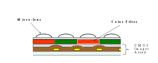
Microlenses - In some pixel designs, the fill factor becomes too small to be effective. For example, if a fill factor in an imager were 25%, this would mean that 75% of the light falling on a pixel would be lost, reducing the pixel's capability. To get around this situation, some CMOS imagers have small lenses manufactured directly above the pixel to focus the light towards the active portion that would otherwise fall on the non-light sensitive portion of the pixel. Microlenses typically can increase the effective fill factor by two to three times.
Color Filter Array (also CFA or just "color filter") - CMOS Pixels are sensitive to light photons but are not, by themselves, sensitive to color. Unaided, the pixels will capture any kind of light, creating a black and white image. In order to distinguish between colors, filters are put on top of a pixel to allow only certain colors to pass, turning the "rods" of the array into "cones". Since all colors can be broken down into an RGB or CMYk pattern, individual primary or complementary color schemes are deposited on top of the pixel array. After being read from the sensor, software takes the different values of the pattern and recombines the colors to match the original picture. There are a variety of different filters, the most popular being the Bayer Filter Pattern (also known as RGBG). Note the large amount of green in the pattern, due to the fact that the eye is most sensitive to color in the green part of the spectrum.
Bayer Color Filter Pattern
Noise - The same as static in a phone line or "snow" in a television picture, noise is any unwanted electrical signal that interferes with the image being read and transferred by the imager. There are two main types of noise associated with CMOS Sensors:
Read Noise (also called temporal noise) - This type of noise occurs randomly and is generated by the basic noise characteristics of electronic components. This type of noise looks like the "snow" on a bad TV reception.
Fixed Pattern Noise (also FPN) - This noise is a result of each pixel in an imager having its own amplifier. Even though the design of each amplifier is the same, when manufactured, these amplifiers may have slightly different offset and gain characteristics. This means for any picture given, if certain pixels are boosting the signal for every picture taken, they will create the same pattern again and again, hence the name.
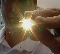
Blooming - The situation where too many photons are being produced to be received by a pixel. The pixel overflows and causes the photons to go to adjacent pixels. Blooming is similar to overexposure in film photography, except that in digital imaging, the result is a number of vertical and/or horizontal streaks appearing from the light source in the picture.
This photo illustrates two undesirable characteristics: blooming, the slight vertical line running from the top to the bottom of the picture and lens flare, the star shape light which is a function of the lens and not the imager.
Optical Format - is a number in inches that is calculated by taking the diagonal measurement of a sensor array in millimeters and dividing by 16. For example, a CMOS Imager that has a diagonal measurement of 4mm has an optical format of 4/16, or ¼".
What Optical Format calculates is the type of lens system that must be used with the imager. In the lens industry, there are standard sets of ¼", ½", ¾", etc. lens systems. By using Optical Format, a user of imagers can use standard, mass-produced (and inexpensive) lens systems rather than having to design and custom build a special lens system. The terms and measurement comes from the days of electron tubes and pre-dates solid-state electronics. Generally speaking, larger optics are more expensive, so a ¼" lens system is less than a 1/3" lens system.
Aspect Ratio - The ratio between the height and width of a sensor or display. It is found by dividing the vertical number of pixels (height) by the horizontal number of pixels (width) leaving it in fractional format.
For example, a pixel with resolution of 640x480 would have an aspect ration of 480/640= ¾.
The most common aspect ratios are ¾ and 9/16. The ¾ aspect ratio is the ratio for computer monitors and TVs. The newer 9/16 aspect ratio is used for High Definition Television (HDTV)
Quantum Efficiency (or QE) - Imagers create digital images by converting photon energy to electrical energy. The efficiency in which each photon is converted to an electron is the imager's quantum efficiency. The number is calculated by simply dividing electrons by photons, or E/P. If no electrons are created, the efficiency is obviously zero, while if each photon creates one electron the efficiency is 100%. Typically, a sensor has different efficiency at different light frequencies, so a graph of the quantum efficiency over the different wavelengths is typically shown:
Dark Current - A situation in CMOS imagers where the pixels fill with thermally created electrons without any illumination. This problem is a function of the manufacturing process and layout and increases with increasing temperature.
The sensors have resolutions from VGA up to 10 Mpixels and some can run at 10,000 frames per second. By Pieter Willems (Product Applications, Engineer, Cypress Semiconductor)
High-speed CMOS image sensors are available in several types for a variety of markets, for use in general purpose, high end or custom high-speed cameras. Such cameras can be used for applications like scientific research, crash tests, high-speed scanning, machine vision and military research; all requiring high frame rate motion capturing.
The sensors have resolutions from VGA up to 10Mpixels and some can run at 10,000 full frames per second. The sensor architecture can consist of two halves, quadrants or one pixel array. The outputs can be parallel analog outputs, one digital 10 bitoutput or digital serial LVDS outputs. The outputs operate at speeds up to 50Msamples/s each, thus realizing a 5.5Gpix/sec pixel throughput. This is the highest reported continuous pixel throughput for an image sensor to date. Image quality is at least 10bit, so after digitization in the camera the data throughput can be 55Gbit/sec. The target applications always require a 6T snapshot pixel with a high sensitivity and high dynamic range. The sensitivity of these image sensors depends greatly on the pixel size. This results in very big pixels and thus very big custom image sensors for some specific applications. Internal multiplexing schemes allow random windowing with increased frame rate. When reducing the window size to a small ROI, the frame rate rises up to 170,000 frames/sec. Most sensors are realized in a 0.25 process.
Recent trends in high speed image sensors
Today CMOS is the technology preferred for high-speed imaging. In today's market we can clearly see three trends in high-speed image sensors; very high speed, feature integration on-chip and generic high-speed imagers.
Pixel rate is the product of resolution and frame rate, and it is advancing by huge proportions. Today we can announce an image sensor of 1024x1024 pixels, working at more than 5000 full frames per second. Taking 10-bit quality into account, this means a total data rate on camera level of 55Gbit/sec. To achieve this extremely high data rate on the sensor level, combined with high image quality and (typically for this type of application) a very high sensitivity, it is important to not only focus on the design with respect to correct schematics, but also making sure the whole layout is well balanced. This means that power lines need to be well-distributed and all parasitic effects, electrical and optical, on each node in the layout should be well controlled. The power budget requires the designs of low power modules to keep within the total power requirement.
Examples of applications for high speed image sensors.
A different trend, in high-speed imaging, is the integration of high-speed ADC's, sequencers, LVDS transmitters and correction algorithms on-chip. These imagers are generally inferior with respect to speed and sensitivity to the imagers above but compensate this with ease-of-use and system integration capabilities. A third type of imagers we see emerging in the market today are generic high-speed imagers. Older (simple) generic imagers with analog outputs or without on-board timing generation are being replaced by faster and more complex image sensors. These imagers allow generic high-speed cameras to be built in a short amount of time.
The pixel
Figure 1 shows the schematic of the pixel used in a typical high-speed image sensor, which is the so-called 6-transitor pixel. Important for this type of image sensor is the pipelined global shutter feature.
The global shutter, in which all pixels start and end light integration at the same time, is very important for a high-speed application to have a well controlled motion blur that is exactly the same for all pixels. This global shutter allows high-speed motion scenes to be frozen by the imager.
Figure 1: The pixel
A typical high-speed capture sequence can be seen in Figure 2 (a small bullet hitting a matchstick). The pipelined feature means that during the readout of the pixel array, the integration of light in the pixel for the next frame is ongoing. This is required to guarantee that the frame rate is independent of the integration time.
Figure 2: Typical high-speed capture sequence (bullet hits match stick)
To obtain the highest possible sensitivity, the photodiode, collecting the photo charge and converting this charge into a voltage, needs to be designed as small as possible to minimize its parasitic capacitance. Additionally, the fill factor of the pixel, meaning the open area in the pixel contributing to the light sensitive area needs to be as large as possible. Both features of a small photodiode and a large fill factor are achieved by implementing the N-well pixel patent, in combination with a P-well opening around the photodiode. Besides a high sensitivity, it is also important to have a pixel storagecapacitor that doesn't give any noise contribution, is well shielded from light and has a low leakage. This pixel architecture gives very good results with respect to storing the pixel signal during readout. The major disadvantage of this structure is the lack of fixed pattern noise correction in the pixel, which has to be done outside the image sensor.
Faster pixel rates
The metric for the speed of an image sensor is the product of resolution and frame rate, this gives the pixel rate of the sensor. In the very high-end, high-speed imaging market, this metric can never be high enough. In this market, customers are willing to build very complex cameras as long as the desired full frame rate is achieved. Figure 3 shows an image of a typical very high-speed application (car crash test).
These very high speeds are only achieved by using parallel analog outputs (up to 128 outputs) that impose an integration challenge for the camera system. The architecture of this type of imager is rather simple; 6T pixels in a pixel array which is optionally divided into quadrants, several parallel high-speed analog busses and parallel output amplifiers to drive the outputs.
Figure 3: High-speed imaging application: Car crash test.
No ADC's, sequencers or other on-chip image processing is present on these chips. The chip-wide analog busses make sure all parallel outputs can be used regardless of the partial image size in the x direction that is readout. This allows boosting frame rate when reading out partial images.
Ghosting An important issue with these very high-speed image sensors is "ghosting" in the x-direction. This is caused by the relative large RC constant of the chip-wide analog busses. As it takes long for the signal on the busses to settle within 10-bit accuracy, a portion of the information of the previous pixel can still be present on the current pixel. In the image this results in ghosting in the x-direction. This type of ghosting is difficult to correct during image post processing.
One technique for addressing this problem is to precharge busses shortly before every new signal. This ensures that all information about previous pixels is destroyed. This technique requires the generation of short precharge pulses. The pulses are used to short the analog bus to ground. Most of these imagers are made as custom products upon request of the customers as there is no real need for this type of very high-speed imagers as a generic product today. Custom specifications can range from VGA to 10Mpixel and from 500 fps to 10000 fps, with data throughput up to 5.5Gpix/s. In figure 4 a typical very high-speed image sensor architecture is shown. Two halves are read-out in parallel with each having 64 parallel analog outputs. This results in a total of 128 high-speed parallel analog outputs!
Figure 4: Architecture of a typical very-high-speed image sensor
Smaller and easier to design with In contradiction with the very complex (and big) camera systems built around the sensors in the previous section, there is an increasing demand in the market for smaller and easier to implement high-speed image sensors.
High-speed imagers are starting to get used in several consumer-like applications such as scanning, vision systems and holographic data storage. The figure below shows a typical holographic data storage application and the imager used in it.
Figure 5: Holographic data storge and its high-speed imager
These applications need a lot of the system functionality to be on-board the image sensor. That is why ADCs, timing generators, image processing and additional output stages are implemented on the chip. For these imagers the level of feature-implementation is equally important as the sensitivity and the speed. Most of these imagers are still made on custom request with specific features that help to simplify the custom high-speed camera design. The figure below gives a typical architecture of this type of high-speed imager. These imagers typically have only one clock input, a few power supplies and some synchronization pins. All other signals to read-out and expose the imager are generated on-chip.
Figure 6: Architecture of a typical high-speed image sensor with a lot of logic and additional features on-board
Generic high-speed image sensors A third kind of high-speed image sensor we see (and have seen the last years) in the market is the general-purpose high-speed image sensor. Its applications range from machine vision cameras to traffic monitoring, scientific motion capturing and crash test inspection. The first generic high-speed image sensors consisted only of parallel analog outputs and had no logic on-board (much like the very high-speed imagers we know today). These days however we see a lot of features being implemented on the chip itself to make sure the imager can be used in a lot of different applications (multiple slope, subsampling, binning, flipping, mirroring, gain, offset, and so on).
Today, high-speed global shutter image sensors are under development that will provide 1.3MPxl at 1000fps. Typically these image sensors have the pipelined snapshot shutter capability and multiple slope capability. The on-board features differ from sensor to sensor.
Figure 7: Variety of applications for which generic high-speed imagers can be used
There are several different types of high-speed image sensors which are needed to meet the needs of different markets today. Very high-speed imaging sensors are purely analog image sensors with very high frame rates and data throughput which require complex -- and therefore mainly custom -- camera design. High-speed imaging sensors with on-board features offer many specific on-board features which assists developers in building these imagers into high-speed cameras which are used for more consumer-oriented applications. Features are implemented upon request of the customer so these are also mainly custom designs.
Finally, generic high-speed image sensors combine the most common features of the image sensors above to create a general-purpose image sensor capable of serving in cameras across a wide range of applications. These image sensors are available today off the shelf. Market trends suggest that on-board features, data rate, and resolution will continue to rise. The real challenge for developers moving into the future will be to combine a very high data rate image sensor with many on-board features such as LVDS and image processing.
About the author Pieter Willems is working as a Product Applications Engineer at the image sensor business unit from Cypress semiconductor. He started his career in the engineering department from Fillfactory and moved to product management before being acquired by Cypress. He can be reached at fpw@cypress.com.
Name: Musa Home: Depok, Jawa Barat, Indonesia About Me: Seorang yg sederhana, moderat, individu serta suka dedikasi dan komitmen dalam semua aspek hidup. Dalam pandanganku sendiri sebagai seorang stabil, bertanggung jawab, percaya diri dan orang penuh kasih yang mempunyai niat baik. Kenangan dari segalanya langkahku merupakan pengalaman berharga dimasa mendatang. Petualanganku dimulai dari pulau “Celebes” yang lebih dikenal dengan Sulawesi. Tepatnya di daerah Gorontalo tempat kelahiran dan masa-masa kecilku bermain dan tumbuh.
Minat yang berkisar akademis terutama hardware system, petualangan. Mengunjungi suatu tempat dan hidup bebas dari “penjajahan” kesenangan penuh kasih.
Bagaimanapun, seorang Purnawarman Musa masih merasakan bahwa aku bukanlah seorang yang sempurna.


